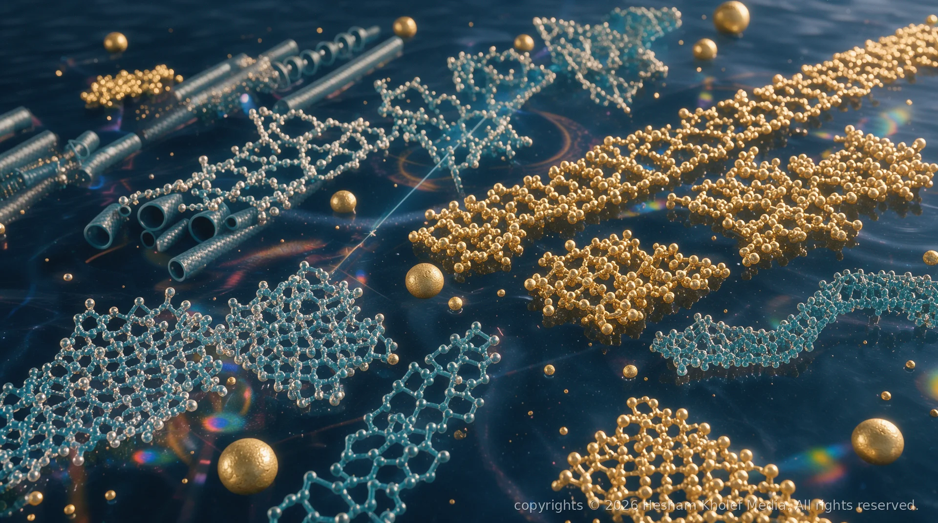
The Nanoscale: Where Physics Changes Its Rules
The prefix "nano" derives from the Greek nanos, meaning dwarf. One nanometer is one-billionth of a meter — roughly the length your fingernail grows in one second. At this scale, the familiar laws of classical physics begin to yield to quantum effects. Surface area dominates volume. Thermal vibrations become violent. Electrons tunnel through barriers. Materials change color, conductivity, and reactivity not because their chemistry changes, but because their geometry does.
Richard Feynman's 1959 lecture "There's Plenty of Room at the Bottom" is rightly cited as the field's conceptual birth. He imagined writing the entire Encyclopedia Britannica on the head of a pin, and manipulating individual atoms. What Feynman could not foresee was that the path to the bottom would not be a straight line of miniaturization, but a convergence of chemistry, biology, and physics — each discipline meeting the others at the nanometer frontier.
What Nanotechnology Is — and What It Is Not
Nanotechnology is: the understanding and control of matter at dimensions between approximately 1 and 100 nanometers, where unique phenomena enable novel applications. It encompasses the synthesis, characterization, and engineering of nanoscale structures — nanoparticles, nanotubes, quantum dots, thin films, and supramolecular assemblies — for specific functions.
Nanotechnology is not: microscopic robots swimming in your bloodstream (the "nanobot" fantasy popularized by fiction). It is not grey goo — self-replicating nanomachines consuming the biosphere (a hypothetical scenario requiring molecular manufacturing capabilities that do not exist). It is not a single technology, but a convergence platform enabling advances across semiconductor fabrication, drug delivery, catalysis, energy storage, and structural materials.
"The nanoscale is not merely a smaller version of the macroscale. It is a distinct regime of matter where the rules are rewritten by quantum mechanics and statistical thermodynamics."
— Hesham Kholef
The Two Paradigms: Top-Down and Bottom-Up

Top-down approaches carve nanoscale features from larger substrates. Photolithography and electron-beam lithography define the modern semiconductor industry, pushing feature sizes below 3 nm in commercial logic chips. This is nanotechnology by attrition — precision removal.
Bottom-up approaches build from atoms and molecules through self-assembly, chemical synthesis, and directed growth. DNA origami folds nucleic acids into prescribed shapes. Colloidal synthesis yields quantum dots with size-tuned emission. Chemical vapor deposition grows carbon nanotubes and graphene. This is nanotechnology by design — leveraging thermodynamics and molecular recognition.
The most powerful advances combine both: directed self-assembly guides bottom-up structures into top-down templates, achieving complexity neither paradigm achieves alone.
Real-World Nanotechnology Today
Nanomedicine: Precision at the Cellular Scale
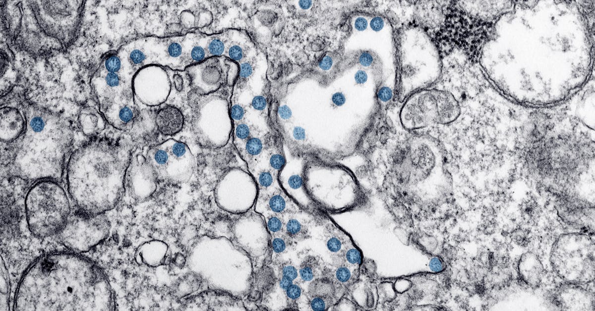
Lipid nanoparticles (LNPs) delivered mRNA vaccines to billions during the COVID-19 pandemic — the most consequential nanotechnology deployment in history. These ~80 nm vesicles encapsulate fragile nucleic acids, evade immune clearance, and fuse with cell membranes to release cargo. Beyond vaccines, LNPs and polymeric nanoparticles are in clinical trials for cancer chemotherapy (Doxil, Abraxane), gene therapy, and crossing the blood-brain barrier.
Gold nanoparticles enable photothermal therapy: infrared light penetrates tissue, nanoparticles absorb and convert it to heat, selectively ablating tumors. Quantum dots provide multiplexed imaging — different sizes emit distinct colors under a single excitation wavelength, mapping multiple biomarkers simultaneously.
Materials That Redefine Performance
Carbon nanotubes and graphene exhibit tensile strengths ~100× steel at one-sixth the density. Commercial composites incorporate them into tennis rackets, bicycle frames, and aircraft components. Yet dispersion, alignment, and interfacial bonding remain stubborn challenges — the "valley of death" between remarkable intrinsic properties and macroscopic composite performance.
Nanocellulose — derived from wood pulp — offers transparency, strength, and biodegradability. It appears in flexible electronics substrates, barrier films for packaging, and lightweight structural foams. The nanoscale fibril network creates a percolating matrix that distributes stress efficiently.
Energy: Storage, Conversion, and Catalysis
Lithium-ion batteries rely on nanoscale engineering: nanostructured anodes (silicon nanowires, graphite particles) accommodate volume expansion during cycling. Solid-state electrolytes use ceramic nanoparticles to suppress dendrite growth. Catalysts for fuel cells and electrolyzers maximize platinum utilization by dispersing it as single atoms or sub-nanometer clusters on high-surface-area supports — reducing cost while maintaining activity.
Perovskite solar cells — solution-processed, tunable bandgap, >25% efficiency — depend on nanoscale grain boundary passivation and interface engineering. Their commercialization hinges on stabilizing these nanostructures against moisture, heat, and light-induced degradation.
Semiconductors: The Engine of the Digital World
Modern logic and memory chips are nanotechnology. The 3 nm process node (a marketing term; actual gate pitches are ~20–30 nm) employs nanosheet transistors — vertically stacked channels surrounded by gate dielectric on all sides. Extreme ultraviolet (EUV) lithography at 13.5 nm wavelength prints these features. Atomic layer deposition (ALD) grows high-κ dielectrics one monolayer at a time. This is nanomanufacturing at scale: billions of transistors per chip, billions of chips per year.
The most impactful nanotechnologies are often invisible — embedded inside vaccines, chips, catalysts, and composites. Their value lies not in being "nano" but in solving problems that larger-scale approaches cannot.
The Hype Cycle: Separating Signal from Noise

The Gartner hype cycle has visited nanotechnology repeatedly. The early 2000s saw "nanotech" appended to everything from socks to tennis balls — often merely marketing conventional microparticles. The U.S. National Nanotechnology Initiative (NNI), launched in 2000, catalyzed genuine research but also attracted opportunistic rebranding.
Red flags for pseudoscience:
- Claims of "molecular manufacturing" or "atomically precise fabrication" available today — these remain theoretical.
- Products asserting "quantum" effects at room temperature without specifying the mechanism (quantum dots exhibit quantum confinement; quantum computing requires cryogenic coherence).
- Fear-mongering about nanoparticles as a unified hazard class — toxicity depends on composition, size, shape, surface chemistry, dose, and exposure route. Titanium dioxide in sunscreen behaves differently from inhaled carbon nanotubes.
Green flags for legitimate advances:
- Peer-reviewed publications with characterized nanomaterials (TEM, SEM, AFM, XRD, DLS, zeta potential).
- Defined synthesis routes with batch-to-batch reproducibility.
- Clear mechanism of action linking nanoscale structure to macroscale function.
- Regulatory pathway engagement (FDA, EMA, EPA) for medical or environmental applications.
Grand Challenges: The Frontier Is Not Where You Think
Scalable Manufacturing with Atomic Precision
Self-assembly yields thermodynamic products; directed assembly yields kinetic products. Bridging the gap — achieving high throughput and atomic precision — is the central manufacturing challenge. Directed self-assembly of block copolymers, DNA-templated fabrication, and scanning-probe lithography are research frontiers; none yet match the throughput of EUV lithography.
Environmental Health and Safety Across the Lifecycle
Nanomaterials enter ecosystems during production, use, and disposal. Their environmental fate — transformation, aggregation, bioaccumulation, trophic transfer — is poorly quantified. Regulatory frameworks struggle with the "same chemical, different size" paradigm. Standardized testing protocols (OECD, ISO) are evolving but lag innovation.
Interfacing Nano with Macro
A nanoparticle suspension is not a device. Integrating nanoscale components into macroscale systems — wiring a single nanotube transistor, sealing a nanofluidic chip, anchoring a catalyst nanoparticle under reaction conditions — demands heterogeneous integration strategies that often dominate cost and failure rates.
Computational Design Inverse to Synthesis
We can simulate nanomaterial properties from first principles (DFT, molecular dynamics). The inverse problem — given a target function, design the structure and synthesis route — remains largely unsolved. Machine learning on materials databases (Materials Project, OQMD, NOMAD) promises data-driven discovery, but experimental validation throughput is the bottleneck.
The Road Ahead: Convergence, Not Revolution
Nanotechnology will not arrive as a singular event. It advances through convergence: biology provides self-assembly blueprints (viral capsids, ribosomes); chemistry provides synthetic diversity; physics provides characterization and theory; engineering provides integration and scale. The next decade will see:
- Programmable matter: DNA origami and protein design creating reconfigurable nanostructures for sensing and computation.
- Single-atom catalysis: Maximizing precious metal utilization while tuning selectivity via coordination environment.
- Neuromorphic nanoelectronics: Memristive devices and spintronic nanostructures emulating synaptic plasticity.
- Nanophotonics for quantum information: Color centers in diamond, quantum dots, and 2D materials as single-photon sources and spin qubits.
Conclusion: A Lens, Not a Label
Nanotechnology is best understood not as a sector but as a lens — a resolution at which the distinctions between disciplines dissolve. The same gold nanoparticle is a catalyst to the chemist, a plasmonic antenna to the physicist, a drug carrier to the biologist, and a process variable to the engineer. Mastery lies in fluency across these languages.
The reality of nanotechnology is neither the dystopian grey goo nor the utopian molecular assembler. It is the quiet, compounding transformation of how we diagnose disease, store energy, compute information, and build materials — one controlled nanometer at a time.
Comments (0)